In 1947, Bardeen, Brattain, and Shockley of Bell Telephone Laboratories demonstrated the transistor function with alloyed germanium and this date is generally recognized as the start of the solid-state semiconductor industry. The era of integrated circuits was inaugurated in 1959, when, for the first time, several components were placed on a single chip at Texas instruments.
These developments resulted in a drastic price reduction in all aspects of solid-state circuitry and the cost per unit of information has dropped by an estimated three orders of magnitude in the last twenty years. This cost reduction been accompanied by a similar decrease in size, and today circuit integration has reached the point where more than a million components can be put on a single chip.
This progress is largely due to the development of glass and ceramic fabrication techinques, single-crystal production processes, and thin-film technologies such as evaporation, sputtering and chemical vapor deposition. These advances were made possible in part by the availability of high-purity molded graphite and its extensive use as molds, crucibles and other components as shown by the following examples.
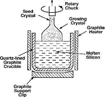
fig.5.14-Czochralski apparatus for crystal growth of silicon
Molded graphite for crystal pulling: Single crystal of silicon, germanium and Ⅲ-Ⅴand Ⅱ-Ⅵ semiconductors are usually produced by the ribbon or the Czochralski crystal-pulling techniques. The later is shown schematically in Fig.5.14. The process makes extensive use of molded graphite, as shown on the figure. The crucible holding the molten material is made of high-purity graphite lined with quartz, and so are the support and the heater. In some cases, the crucible is coated with pyrolytic boron nitride deposited by chemical vapor deposition.
Other molded graphite applications in semiconductor processing: The following is a partial list of current applications of molded graphite is semiconductor processing:
— Boats and assemblies for liquid-phase epitaxy
— Crucibles for molecular-beam epitaxy
— Susceptors for metallo-organic CVD
— Wafer trays for plasma-enhanced CVD
— Shields, electrodes, and ion sources for ion implantation
— Electrodes for plasma etching
— Barrel-type wafer holders for epitaxial deposition.
— Liners for electron-beam evaporation
— Resistance-heated jigs for brazing and glass-to-metal sealing
— Electrodes for polycrystalline-silicon deposition
— Boats for reduction heating of germanium oxide
— Anodes for power tubes and high-voltage rectifiers
In some of these applications, it is necessary to coat the surface of the molded graphite with a more inert coating such as pyrolytic graphite, boron nitride or silicon carbide, to prevent contamination and reaction with the graphite at high temperature. The coating is usually done by CVD as reviewed in Ch.7.