For the present investigation we have used freshly cleaved highly oriented pyrolytic graphite HOPG. By peeling off the surface layers using scotch tape, we were able to obtain ribbons and terraces with step edges. The peeling off process dislocates the layers laterally and vertically. We have studied only monolayer steps to avoid complexity in the electrical analysis. Commercial AFM was used for the present investigation. Cantilevers used were platinum coated with a radius of curvature of the tip -35nm and the cantilever elastic constant 0.1 N/m. For imaging in the contact mode the normal force between the surface and the tip was kept around -25nN. The sample was biased with 10 to 15 mV for measuring the local conductance of the sample surface with the conducting tip. By measuring the tip-sample contact conductance during the scanning process, we measure the local conductance of the sample surface. For purely ohmic contacts, the I-V is of the typical spreading resistance from
R spreading=ρ/2a (1)
Where is the mean resistivity of the tip-sample contact and a is the contact area. All the measurements were conducted at room temperature and ambient conditions. For topographic images we have only subtracted the linear line fit along the scan direction from the scanned images and presented without any further filteration or averaging. For the conductance map we show only the raw results without any processing.
In Fig.2(a) and 2(b) we show the topographic image and local conductance map of a freshly cleaved HOPG sample. We see that the contrast in the local conductance map is much better than the topographic image. Each separate graphite ribbons can be easily distinguished in the local conductance map. The local conductance image of the HOPG sample clearly indicates that the conductivity of these ribbons are different since the conductance was mapped in a constant force mode. Hence the tip-sample contact conductivity measured is a direct measure of the local conductivity of the sample and is not due to change in the area of the contact. Since we have used a 35nm radius of a curvature tip, we can safely say that the tip-sample contact area is limited by this and will be less than this value.

Fig.2-atomic force microscopic image
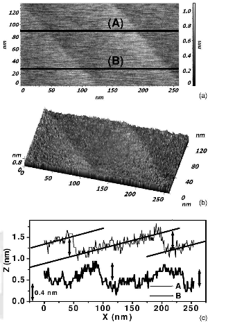
Fig3.(a)Togpgraphic 2D (b)3D images(c) two height profiles
In Fig3(a) and 3(b) we show topographic two-dimensional (2D) and three-dimensional (3D) images of a selected region containing two monolayer steps/edges on the surface of the HOPG sample. In Fig.3(c) we show two line profiles marked in Fig.3(a) as A and B. We can clearly see the step heights to be around -0.4 nm close to the
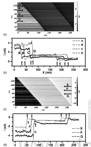
Fig.4-local conductance map of step of Fig.3
reported c-axis value of 0.35nm for the HOPG sample. In Figs. 4(a) and 4(c) we show the local conductance map of these steps for the forward and the reverse biased condition, respectively. We can clearly see the contrast inversion and reversal of the current direction on reversing the bias. The higher current is indicated by the brighter shade and the lower current by the darker shade in the forward bias condition and the scale is shown on
the right-hand side of the image. In the reverse bias condition the higher negative current value is indicated by the darker shade and low negative value is shown as the brighter shade. In Fig.4(a) the brightest layer is the top layer and the darkest is the lowest layer. A detail discussion on the difference in the current contrast will be discussed in the next section. In Figs 4(b) and 4(d) we show the line profile of the current along the lines marked in the conductance images. We see distinct changes in the current profile at the step edges in comparison to the height change in the topography. This clearly demonstrates why the contrast is better in the conductivity map than the topographic map. At the closer look we see distinct dips in the current occurring at the lower layers at each of the interface of the step edges. Since the conductance depends on the local electron density, the dip in the conductance of the lower layers near the step edge is the manifestation of the depletion of the local electron density. This feature has never been observed earlier to our knowledge using either STM or AFM.